

WAVEELECA ENGINEERING
RF • Antennas • PCB Design • AI • Robotics • R&D
Engineering the Intelligent Future
PhD-led RF, microwave, antenna, high-speed PCB, AI and robotics engineering, taking your product from concept and simulation to tested, manufacturing-ready hardware.
Who we are
Welcome to WAVEELECA ENGINEERING
WAVEELECA ENGINEERING is an advanced engineering company based in Abbottabad, Pakistan, serving clients worldwide. Our PhD-led team combines research depth with practical design experience across RF and microwave systems, antennas and phased arrays, high-speed PCB design, embedded systems, and artificial intelligence. We turn complex technical requirements into reliable, manufacturing-ready solutions.
What drives us
Our Mission & Vision

Our Mission
To deliver reliable, research-driven engineering solutions in RF, antennas, electronics and intelligent systems — helping clients turn complex technical ideas into tested, manufacturing-ready products.

Our Vision
To become a trusted global engineering partner from Pakistan, recognised for technical excellence in wireless, microwave and intelligent hardware technologies.
Our expertise
What We Do
End-to-end engineering services across six core disciplines.
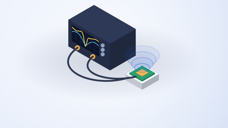
RF & Microwave Engineering
RF front-ends, microwave/mmWave circuits, phase shifters and system-level design.
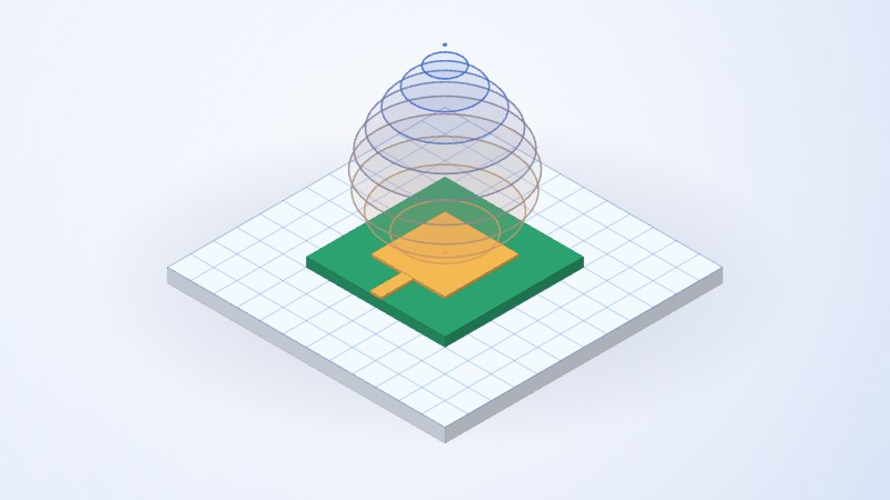
Antennas & Phased Arrays
Phased, conformal, MIMO and reconfigurable antennas with beam steering.
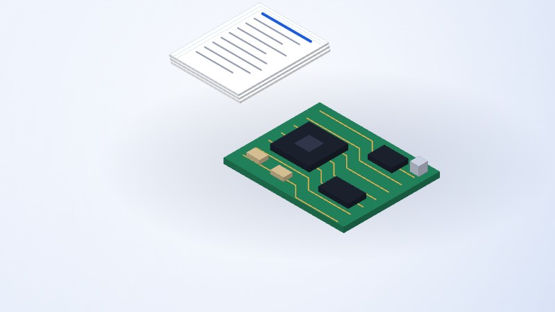
PCB Design
Multilayer, high-speed and RF PCBs — FPGA, PCIe and power boards, ready for fabrication.

Artificial Intelligence
Machine-learning models and intelligent algorithms for engineering applications.

Robotics & Embedded Systems
Firmware, sensors, control electronics and hardware integration.

Research & Development
Electromagnetic simulation, prototyping and experimental validation.
Our strengths
Why Choose WAVEELECA
Research depth, practical engineering and reliable delivery.

PhD-Led Expertise
Led by researchers with doctorates in antennas, electromagnetics and electronic engineering, backed by more than 28 international publications.
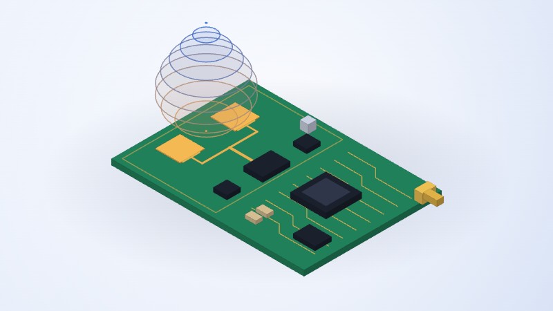
Simulation-Driven Design
Every design is verified in CST, HFSS, ADS and circuit simulators before fabrication, reducing technical risk and costly redesigns.
Manufacturing-Ready Output
Complete Gerbers, BOMs and design documentation, prepared for smooth fabrication and assembly with your chosen manufacturer.

Global Client Support
Clear communication and dependable delivery for clients across the USA, Europe and the Middle East, wherever you are based.
Portfolio
Featured Engineering Projects
Selected research and engineering work from our team.
Antennas
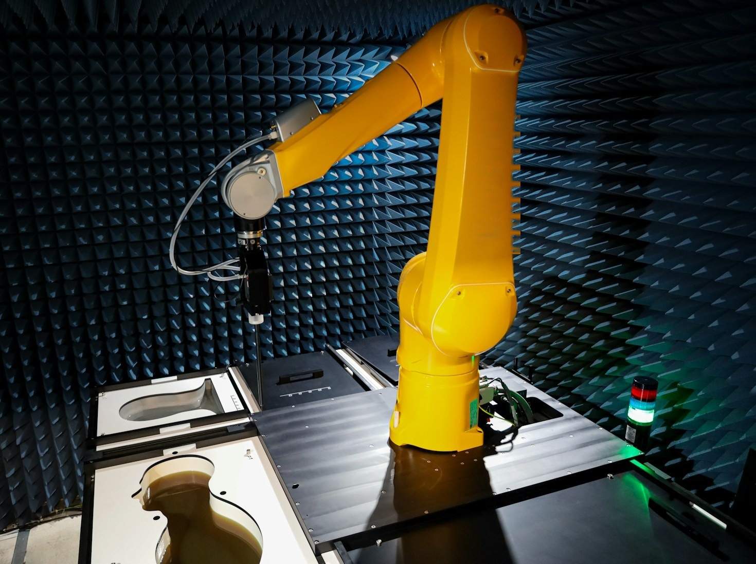
Conformal Beamforming Antenna Array
Cylindrical and wedge-shaped beamforming arrays for aerial platforms, covering modelling, fabrication and anechoic-chamber measurement.

Phased Arrays
Flexible Phased Array with CRLH Phase Shifters
Conformal phased array steered by CRLH metamaterial phase shifters with embedded magnetic particles, published in IEEE Access (2024).
PCB Design
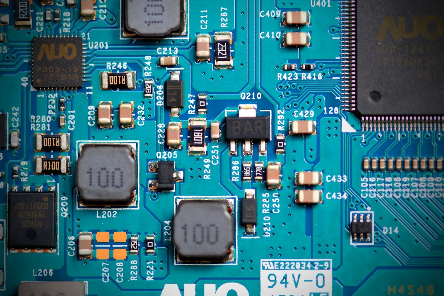
High-Speed FPGA & PCIe Carrier Boards
Multilayer high-speed FPGA and PCIe carrier boards with controlled-impedance routing and signal-integrity review, delivered manufacturing-ready.
Delivered · USA
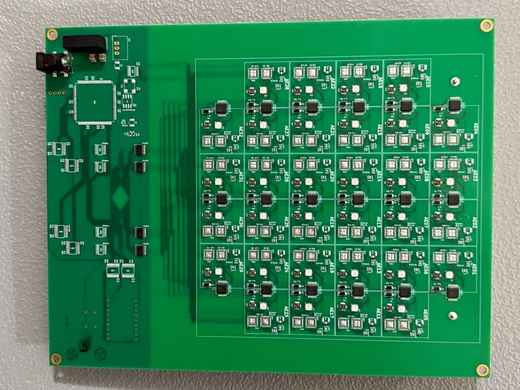
Wi-Fi 8 PCB Antenna
32 Patch Element 6 GHz Phased Array. A dual-polarized antenna array (DPARx) designed and delivered for a USA company, now operating successfully.
How we work
Our Engineering Approach
Design → Simulation → Prototyping → Testing
01
Design
Requirements analysis, system architecture and detailed schematic or antenna design, agreed before work begins.
02
Simulation
Full-wave electromagnetic and circuit simulation to optimise performance and resolve design issues before fabrication.
03
Prototyping
PCB layout, fabrication-ready files, fabrication support and prototype assembly, coordinated with your manufacturer.
04
Testing
S-parameter, gain and radiation-pattern measurement, validation and documentation against the agreed specification.
Our track record
Key Achievements
Verified experience behind every project.
8+
Years of RF & antenna research experience
28+
Research publications by our Technical Director
2
PhD-qualified engineering experts
100%
Client satisfaction on freelance PCB projects
Have an Engineering Project? Let’s Build It Together.
Share your requirements with our team and receive a tailored technical proposal.